
The global semiconductor landscape has officially entered the 2-nanometer (2nm) era, marking a profound architectural evolution in computing. This milestone, achieved through rigorous innovation by industry giants like TSMC, Samsung, and Intel, signifies more than just smaller transistors; it represents the foundational engine for the next generation of artificial intelligence. As we navigate 2026, the transition to 2nm process technology is enabling “Agentic AI” – autonomous systems capable of complex reasoning and multi-step problem-solving – to move from the confines of centralized data centers directly onto consumer devices and sophisticated robotics. This shift dismantles the long-feared “physics wall” that many believed would stall Moore’s Law at the 3nm node, paving the way for unprecedented power efficiency and compute density. The implications reverberate across mobile computing, advanced AI applications, and geopolitical strategy, signaling a new chapter in technological advancement where innovation at the atomic scale reshapes our digital future.
In Brief: Inside the 2nm Era
- The 2nm threshold has been crossed by TSMC, Samsung, and Intel, driving a significant architectural shift in computing.
- This advancement is crucial for “Agentic AI,” enabling complex AI to run on consumer devices and robotics.
- The industry has adopted Gate-All-Around (GAA) architecture, replacing FinFET, to overcome previous physical limitations.
- TSMC’s N2 node offers substantial performance and power efficiency gains through its Nanosheet FET design.
- Intel’s 18A node, featuring PowerVia and RibbonFET, showcases aggressive innovation in power delivery.
- Samsung’s SF2 node, building on its earlier MBCFET experience, provides unique design flexibility despite ongoing yield optimization.
- Major tech players like Apple, NVIDIA, Microsoft, and AMD are leveraging 2nm to enhance their AI and mobile product lines.
- The widespread adoption of High-NA EUV lithography is a key enabler and indicator of national technological standing.
- The 2nm era signals a shift towards “Physical AI,” integrating advanced AI models into real-world applications like robotics and autonomous vehicles.
- Future roadmaps already target 1.4nm (A14) and the “Angstrom Era,” focusing on 3D integration and sustainable manufacturing.
The Dawn of 2nm: A Paradigm Shift in Computing
The global semiconductor industry has officially entered a transformative period, with the widespread adoption of 2-nanometer process technology. This move, which began to reach high-volume manufacturing in late 2025 and early 2026, represents the most significant architectural shift in over a decade. It’s not merely an incremental improvement; it’s a fundamental reimagining of how transistors operate at the atomic scale, driven by the insatiable demands of artificial intelligence. Specifically, this leap powers the rise of “Agentic AI”—intelligent systems capable of not just processing information, but understanding context, planning multi-step solutions, and executing them autonomously across various environments. This newfound capability fundamentally changes what is possible for mobile devices and embedded AI applications.
For years, experts debated the sustainability of Moore’s Law, anticipating a “physics wall” that would halt further miniaturization. The successful transition to 2nm, however, has effectively dismantled this barrier, allowing for unprecedented levels of power efficiency and compute density. This means that sophisticated AI models, once confined to massive data centers, can now reside and operate directly on personal devices, from the latest smartphones to advanced robotics. The move away from the FinFET (Fin Field-Effect Transistor) architecture, which had been the industry standard since 2011, is central to this revolution, making way for more advanced transistor designs that fundamentally alter performance envelopes. This allows for a deeper integration of AI into our daily lives, transforming everything from personal assistants to advanced industrial automation, as highlighted in discussions around industrial robotics and smart systems.
Engineering at the Atomic Scale: The Gate-All-Around Revolution
The core of the 2nm breakthrough lies in the industry-wide adoption of Gate-All-Around (GAA) transistor technology, moving beyond the limitations of FinFETs. TSMC, a leader in foundry services, has achieved volume production of its N2 node, primarily at its Hsinchu and Kaohsiung fabs. Their “Nanosheet FET” design is a marvel of precision, completely surrounding the transistor channel with the gate on all four sides. This intricate design choice results in an impressive 75% reduction in leakage current compared to previous generations, directly translating into either a 10-15% performance increase at the same power level or a remarkable 25-30% reduction in power consumption for equivalent speeds. Such efficiencies are critical for mobile devices where battery life is paramount and for AI accelerators running complex algorithms continuously.
Intel has taken an aggressive and distinct technical approach with its Intel 18A (1.8nm-class) node, aiming to regain its competitive edge. While other foundries focused on nanosheet structures, Intel introduced “PowerVia,” the first implementation of Backside Power Delivery in the industry. By routing power wiring to the back of the wafer, separate from signal wiring, Intel has dramatically reduced “voltage droop” and boosted power delivery efficiency by approximately 30%. Combined with their “RibbonFET” GAA architecture, Intel’s 18A node has allowed the company to achieve technical parity and, by some measures, a lead in power delivery innovation that TSMC aims to match by late 2026. This innovative strategy from Intel is reshaping the competitive landscape and underscores the intense innovation happening at this scale, a dynamic often explored when discussing the foundry war.
Samsung, not to be outdone, leveraged its “first-mover” status in GAA technology, having introduced its Multi-Bridge Channel FET (MBCFET) at the 3nm stage. This early experience has granted Samsung’s SF2 node unique design flexibility, allowing engineers to fine-tune the width of nanosheets. This customization optimizes chips for diverse applications, from ultra-low-power mobile processors to high-performance AI accelerators. While Samsung’s yield rates are still maturing compared to TSMC’s established figures, their SF2P process is already attracting significant interest from major high-performance computing clients, indicating a strong future for their advanced manufacturing capabilities.
The Foundry War: Who’s Winning the AI Chip Race?
The arrival of 2nm technology is intensifying the strategic positioning of the world’s leading tech companies, as the race for AI supremacy heats up. Apple, known for its meticulous supply chain management, has reportedly secured over 50% of TSMC’s initial 2nm capacity. This exclusive access is foundational to its new A20 and M6 chips, powering the latest iterations of the iPhone and Mac. These chips feature Neural Engines that are 2-3 times faster than their 3nm predecessors, enabling “Apple Intelligence” to perform advanced multimodal reasoning entirely on-device. This on-device processing offers a critical advantage in privacy-focused AI applications, setting a new benchmark for integrated performance and efficiency in mobile computing.
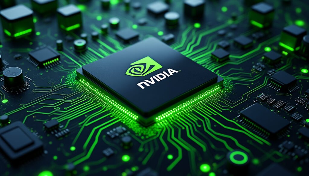
NVIDIA has capitalized on the 2nm transition with the launch of its “Vera Rubin” supercomputing platform. The Rubin R200 GPU, built on TSMC’s N2 node, contains an astonishing 336 billion transistors. It is specifically engineered to handle trillion-parameter models with a remarkable 10x reduction in inference costs. This has democratized large language model (LLM) execution, allowing tech giants like Microsoft and Amazon to significantly scale their AI services more efficiently. Microsoft, for instance, has committed to Intel’s 18A node for its custom silicon strategy, signing a multibillion-dollar deal to manufacture its “Maia” series of AI accelerators in Intel’s domestic fabs. This demonstrates a strategic shift towards diversified foundry sourcing to mitigate geopolitical risks and leverage unique technical advantages, as seen with the AI chip breakthrough.
For AMD, the 2nm era presents a significant opportunity to challenge NVIDIA’s dominance in the data center market. Their “Venice” EPYC CPUs, leveraging 2nm architecture, offer up to 256 cores per socket, providing the thread density necessary for the massive “sovereign AI” clusters being developed by national governments and large enterprises. The competition among foundries to secure long-term contracts with hyperscalers is now at a fever pitch, with clients increasingly seeking “foundry diversity” to hedge against potential disruptions in East Asian production hubs. This intense rivalry is pushing the boundaries of what is possible in high-performance computing, fostering rapid innovation across the entire ecosystem.
Beyond Transistors: Global Implications of the 2nm Era
The strategic importance of the 2nm race extends far beyond corporate balance sheets; it is intricately linked to national security and global economic stability. The successful deployment of High-NA EUV (Extreme Ultraviolet) lithography machines, exclusively manufactured by ASML, has become the de facto metric of a nation’s technological prowess. These sophisticated machines, each costing upwards of $380 million, are the only tools capable of printing the minuscule features required for sub-2nm chips. Intel’s early adoption of High-NA EUV has sparked a manufacturing renaissance within the United States, particularly at its “Silicon Heartland” sites in Oregon and Ohio, bolstering domestic production capabilities and supply chain resilience.
This technological transition also signifies a crucial shift in the AI landscape, moving from purely “Generative AI” to “Physical AI.” The extraordinary efficiency gains offered by 2nm technology enable complex AI models to be deeply embedded within robotics and autonomous vehicles without the need for cumbersome battery arrays or constant cloud connectivity. Imagine a world where robots can perform intricate tasks with real-time, on-device intelligence, greatly reducing latency and enhancing reliability. However, the escalating cost of building these advanced fabs, now exceeding $30 billion per site, raises concerns about a widening “digital divide.” Only the largest tech giants can afford to design and manufacture at these cutting-edge nodes, potentially stifling smaller startups that struggle to keep pace with the increasing “cost-per-transistor” for the most advanced hardware, impacting the broader ecosystem of AI chip challengers.
Compared to previous milestones, such as the transition to 7nm or 5nm, many industry experts view the 2nm breakthrough as the “Atomic Era” of semiconductors. We are now engineering at a scale where quantum tunneling and thermal noise are not just theoretical concepts but primary engineering obstacles. The shift to GAA was not merely an upgrade; it necessitated a complete reimagining of the fundamental switch at the core of computing. This era challenges engineers to innovate with exotic materials and novel designs, pushing the boundaries of physics itself to continue the relentless march of technological progress.
The Road Ahead: 1.4nm and the Angstrom Horizon
Even as 2nm technology solidifies its position in mainstream production, the semiconductor industry is already charting the course for the “Angstrom Era.” The roadmap towards 1.4nm (A14) is being actively developed by TSMC, Intel, and Samsung, with targets set for 2027 and 2028. Intel, for example, is already conducting pilot testing for its 14A process, with ambitions to be the first to leverage High-NA EUV for mass production on a global scale. These future nodes are expected to integrate even more exotic materials and embrace sophisticated “3D heterogeneous integration,” where memory and logic components are stacked in complex vertical architectures. This innovative stacking aims to further reduce latency and increase overall system performance, addressing the growing computational demands of future AI applications.
The next two years are anticipated to witness the significant rise of “AI-designed chips,” where 2nm-powered AI agents are employed to optimize the intricate layouts of 1.4nm circuits. This creates a recursive loop of technological advancement, where AI itself becomes a tool for accelerating chip design and efficiency. However, alongside these incredible advancements, the industry faces persistent challenges. The soaring cost of electricity required to power these colossal fabrication plants and their substantial environmental impact are pressing concerns. Experts predict that future victories in this technological race will not only depend on who can create the smallest and most powerful transistor but also on who can achieve this with the highest degree of environmental sustainability and yield efficiency, ensuring a responsible and robust future for advanced computing. For those interested in the foundational elements powering these innovations, understanding the battle for AI supremacy provides crucial context.